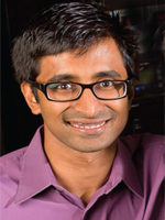
Dr. Ganesh Balakrishnan is a Professor in the Department of Electrical and Computer Engineering at the University of New Mexico (UNM), part of the School of Engineering. His research focuses on III-Sb compound semiconductors, molecular beam epitaxy (MBE), and optoelectronic devices. He leads the Center for High Tech Materials and has contributed over 60 peer-reviewed publications, 30 conference presentations, and multiple patents. His work emphasizes low-defect epitaxy for advanced semiconductor integration. Education: PhD in Optical Science and Engineering (UNM, 2006), MS in Electrical Engineering (University of Toledo, 2001), and BS in Electronics and Communications Engineering (University of Madras, 2000). Research interests include mismatched semiconductor epitaxy, narrow-gap devices, and photovoltaic systems. His recent studies address high-brightness photonic crystal surface-emitting lasers (PCSELs), quantum dot-based single-photon emitters, and radiation-resistant materials. He collaborates on metamorphic substrates and semiconductor membranes for electromagnetic interference shielding. Dr. Balakrishnan’s lab, the Center for High Tech Materials, focuses on advanced semiconductor fabrication and device applications. His work bridges materials science, photonics, and optoelectronics, with applications in defense, energy, and space technologies.
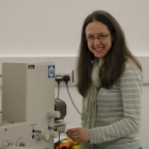
Prof Rachel Oliver is a Professor of Materials Science at the University of Cambridge , affiliated with the Department of Materials Science & Metallurgy . She serves as Director of the Cambridge Centre for Gallium Nitride and Chief Scientific Officer of the spinout company Poro Technologies . Education: MEng, University of Oxford DPhil, University of Oxford Her research focuses on the characterization and engineering of GaN-based materials for optoelectronic and electronic devices. Key areas include defect analysis in nitride semiconductors, quantum dot development for single-photon sources, and porous GaN applications. She employs advanced techniques like atom-probe tomography , cathodoluminescence , and electron microscopy to study structure-property relationships. Recent publications highlight trends in solar cell efficiency optimization, quantum well dynamics, and multi-microscopy characterization of defects. Her work addresses challenges in nitride materials, such as efficiency droop and defect passivation. Scientific Awards: Fellow of the Royal Academy of Engineering (FREng) Rachel Oliver leads the Cambridge Centre for Gallium Nitride, a key player in the EPSRC National Epitaxy Facility , providing nitride materials to UK academics. Her team collaborates on projects involving quantum cryptography , power electronics , and novel device concepts .
Minjoo Lawrence Lee is a Professor in the Department of Electrical and Computer Engineering at the University of Illinois Urbana-Champaign's Grainger College of Engineering. He serves as Director of the Holonyak Micro and Nanotechnology Laboratory (HMNTL) since January 2023 and holds the Intel Alumni Endowed Faculty Scholar position. Previously, he was Associate Professor at UIUC (2016-2021) and Assistant/Associate Professor at Yale University (2008-2016). Lee earned his Sc.B. from Brown University in 1998 and Ph.D. from MIT in 2003. His research focuses on developing materials and devices for integrated photonics, solar energy, electronics, and sensing, with particular expertise in III-V and III-N compound semiconductors. His work emphasizes direct growth of these materials on silicon substrates to enable heterogeneous integration and scalability. Lee's research group explores photonic technologies, quantum technologies, and solar energy conversion, with special emphasis on III-V solar cells on silicon, visible lasers on silicon, and advanced epitaxial growth techniques. His recent work has achieved record efficiencies in III-V/Si tandem solar cells and visible lasers on silicon substrates. His publication record shows a strong focus on advancing solar cell technology, particularly wide-bandgap III-V materials for multi-junction solar cells. His most recent 2025 review in Applied Physics Reviews highlights the state of the art in wide-bandgap III-V solar cells, which play a crucial role in high-efficiency multi-junction solar cells by efficiently converting visible photons into electrons at high voltage. Optica Fellow (2025) for pioneering contributions to molecular beam epitaxy growth of III-V optoelectronic devices on silicon Intel Faculty Scholar (2023) Dean's Award for Excellence in Research (2021) IBM Faculty Award (2016) NSF CAREER Award (2010) Lee has mentored numerous students who have received multiple best presentation awards at major conferences. His group is expanding its capabilities with III-nitride growth starting in 2025. He teaches courses including ECE 210 (Analog Signal Processing), ECE 211 (Analog Circuits & Systems), ECE 329 (Fields and Waves I), and ECE 444 (IC Device Theory & Fabrication), and has been repeatedly ranked as excellent by students.
Professor Madan Niraula serves in the Department of Electrical and Electronic Engineering at Nagoya Institute of Technology's Graduate School of Engineering, where he leads semiconductor radiation detector research. His laboratory (SMD Lab) focuses on developing advanced materials for medical and industrial imaging applications. Doctor of Engineering, Shizuoka University (2000) Master's Degree, Shizuoka University (1997) B.E., Bangladesh University of Engineering and Technology (1993) B.Sc. in Biology, Tribhuvan University, Nepal (1987) Professor Niraula's research centers on semiconductor radiation detection technology, with particular expertise in CdTe crystal growth and perovskite-based X-ray detectors . His work addresses critical challenges in dislocation engineering, MOVPE epitaxy, and detector performance optimization for medical imaging applications. Recent investigations focus on halide perovskite single crystals and advanced annealing techniques to enhance radiation detection capabilities. Analysis of his publication record reveals consistent advancement in semiconductor detector technology, with increasing emphasis on perovskite materials since 2020 while maintaining core expertise in CdTe/Si heterostructures. His research demonstrates strong industry-academia collaboration through multiple patents and NEDO-funded projects. The Electrical Science and Engineering Promotion Awards (2012) 2004 Tokai Academic Promotion Prize Japan Society of Applied Physics Spring Meeting Award (2002) Professor Niraula has secured continuous research funding since 2003, including competitive Japanese scientific grants (Kakenhi) and industry partnerships with organizations like NEDO and the Nakatani Foundation. His laboratory maintains active collaborations with Brookhaven National Laboratory and international research institutions, evidenced by his committee roles in IEEE, SPIE, and the Applied Physics Society. Current projects focus on developing photon-counting X-ray detectors and improving CdTe growth techniques for medical imaging applications.
Dr. Fabien Massabuau is a Senior Lecturer in the Department of Physics at the University of Strathclyde, where he joined as a Chancellor's Fellow in September 2019. His research focuses on wide bandgap semiconductors for ultraviolet optoelectronic devices, with particular emphasis on α-Ga 2 O 3 and h-BN. Prior to his position at Strathclyde, Dr. Massabuau completed his PhD (2011-2015) and served as a post-doctoral researcher (2015-2019) at the Department of Materials Science and Metallurgy at the University of Cambridge. During his time at Cambridge, he developed a "multi-microscopy" methodology to study nanoscale features across multiple imaging platforms (AFM, SEM-CL, TEM), advancing understanding of defects in III-Nitride materials. Dr. Massabuau's research interests span wide bandgap semiconductors, ultraviolet optoelectronics, and the fundamental relationship between nanostructure and optical properties in semiconductor materials. His work has significant applications in UV photodetection, water quality monitoring, and radiation-resilient sensor technologies. He actively investigates gallium oxide variants (α, β, and κ phases) and hexagonal boron nitride, focusing on defect engineering and performance optimization for practical device applications. His recent publications demonstrate a strong focus on gallium oxide materials systems, with particular attention to crystal structure-property relationships, defect characterization, and device performance metrics. The research shows increasing integration of computational approaches with experimental characterization to optimize material properties. Dr. Massabuau has received numerous prestigious awards: Materials Young Investigator Award (2025) 2024 Emerging Leader in J. Phys. D: Appl. Phys. Nanoscale 2022 Emerging Investigator European Crucible Seed Funding Award for Nanostructure-enhanced Gallium Oxide UV photodetectors (2021) European Crucible Seed Funding Award for Developing new tools for evaluating nanoscale biological interactions (2021) 2021 Emerging Leader in J. Phys. D: Appl. Phys. As a Principal Investigator, Dr. Massabuau leads multiple research projects including "Gallium Oxide Optoelectronic Devices for Water Pollution Sensing (GOOD-Water)" and "Tuneable radiation-resilient (AlGa)2O3 UVC photodetectors." He serves on the committee for Doctoral Researcher Awards and is a member of the editorial board for SN Applied Sciences. With over 40 peer-reviewed articles, 2 book chapters, and 1 mobile application to his name, his work has accumulated more than 600 citations. Dr. Massabuau actively participates in the semiconductor research community through conference organization (including the upcoming "Ultra-wide bandgap oxides 2025" conference) and as an invited speaker at international venues focusing on defects in α-phase Ga 2 O 3 . His research group continues to advance the understanding and application of wide bandgap semiconductors for next-generation optoelectronic devices.
Shyh-Chiang Shen is a Full Professor in the School of Electrical and Computer Engineering at the Georgia Institute of Technology. He holds affiliations with the Institute of Electronics and Nanotechnology (IEN), the Center for Compound Semiconductors (CCS), the Package Research Center (PRC), and the Georgia Electronic Design Center (GEDC). His research focuses on wide-bandgap semiconductor (WBG) technologies, particularly III-nitride devices for optoelectronics and power electronics. Dr. Shen earned his B.S. and M.S. in Electrical Engineering from National Taiwan University (1993–1995) and his Ph.D. from the University of Illinois at Urbana-Champaign (UIUC) in 2001. His career includes roles at Xindium Technologies (2000–2004) developing InP-based optoelectronic integrated circuits and GaAs MESFETs. At Georgia Tech since 2005, he leads the Semiconductor Research Laboratory (SRL), where his team advances GaN-based power electronics and UV optoelectronics. His research interests span high-sensitivity UV photodetectors, III-nitride coherent light emitters, high-power GaN transistors, and GaN-based integrated circuits. Key projects include first demonstrations of GaN HBTs, Geiger-mode UV APDs, and monolithically integrated 40 Gb/s optical receivers. Dr. Shen’s work has yielded 8 U.S. patents, over 170 refereed publications, and 5 book chapters. His scientific awards include the 2010 Richard M. Bass Outstanding Teacher Award (Georgia Tech senior class vote), 2011 Outstanding Junior Faculty Award, and 2012 Undergraduate Research Mentor Award. He is an OSA Fellow and IEEE Senior Member. His lab, BH 256, features a class-1,000 cleanroom with advanced equipment (e.g., e-beam evaporator, contact aligner, rapid thermal annealing). Collaborations with material growth groups aim to bridge research and commercial applications in III-N devices for power electronics and optoelectronics.
Jochen Bruckbauer is a Research Fellow in the Department of Physics at the University of Strathclyde, affiliated with the Semiconductor Spectroscopy & Devices Group. He holds a PhD from the University of Strathclyde (2013) and a Diplom (Master of Science equivalent) from the Technical University of Munich. His research focuses on optical characterization of III-nitride semiconductors, particularly their applications in solid-state lighting and optoelectronic devices. Key techniques include cathodoluminescence hyperspectral imaging and electron channelling contrast imaging. He collaborates with the Department of Pure and Applied Chemistry on hybrid organic/inorganic LEDs. Research Interests: Optical spectroscopy, electron microscopy of semiconductors, III-nitride nanostructures, dislocation analysis, and LED development. Techniques employed include CL hyperspectral imaging, photoluminescence, and EBSD. Professional Activities: Invited speaker at RMS EBSD meetings (2025), XVIIIth International Conference on Electron Microscopy (2024), and MRS Fall Meeting (2023). Active in grant-funded projects, including the IAA Proof of Concept for semiconductor device measurement (2024–2026) and EPSRC-funded initiatives. Awards: Outstanding Poster Award (ICNS13, 2019), Fred Stern Memorial Prize (2014), and Best Poster Award (Strathclyde Research Day, 2011). Labs/Teams: Leads projects on semiconductor characterization and collaborates across disciplines, leveraging advanced microscopy facilities. His work contributes to sustainable lighting solutions aligned with UN SDGs.
Georgakilas Alexandros is a Professor in the Department of Physics at the University of Crete , where he has been since 1995. His research focuses on applied physics and materials science, particularly III-V semiconductor heterostructures and nanostructures for advanced electronic and optoelectronic devices. He has contributed to understanding material properties, structural-electronic correlations, and device integration. Research Interests : Molecular Beam Epitaxy (MBE) of III-V semiconductors, GaN-based heterostructures on Si and diamond substrates, quantum wells, nanowires, and their applications in high-electron mobility transistors (HEMTs), power electronics, and optoelectronics. His work also investigates defect analysis, strain effects, and polarization-dependent properties. Articles Trends : His publications emphasize semiconductor device modeling, GaN/InN-based heterostructures, nanostructure fabrication, and material characterization under stress. Key themes include defect impact on mobility, integration challenges, and quantum confinement effects. Education : B.A. in Physics (1984), University of Patras Ph.D. in Physics (1990), University of Crete (research on III-V semiconductors at Thomson-CSF/LCR and EKEK/IHDL) Career : 1984-1995: Research Assistant/Contract Researcher at FORTH-IEL 1987: Thomson-CSF, Paris 1991-1992: University of Maryland, USA 1995: Assistant Professor, University of Crete 2002: Associate Professor 2010: Professor 2019-2023: Chair of the Department of Physics
Vidar Skogvoll serves as a Senior Lecturer at the Centre for Teaching and Learning in Science (KURT) within the Department of Physics at the University of Oslo's Faculty of Mathematics and Natural Sciences. His work bridges computational physics research and innovative science education methodologies, with particular focus on integrating generative artificial intelligence into academic instruction. He maintains active roles in both the Interface Dynamics in Geophysical Flows (EarthFlows) research group and the Center for Computing in Science Education (CCSE). Skogvoll's research spans computational physics (specializing in topological defects and phase field crystal modeling) and AI-enhanced education . His ComFiT library represents significant contributions to open-source scientific software, while his educational projects explore scaffolding techniques for student use of large language models. He actively develops resources through llmteaching.com and comfitlib.com , and produces educational content through dual podcast platforms focusing on science pedagogy and popular science. His publication record demonstrates consistent output in high-impact physics journals including Physical Review B, Journal of Mechanics and Physics of Solids, and Modeling and Simulation in Materials Science and Engineering. The research exhibits strong methodological continuity in computational approaches to material defects while showing recent expansion into AI applications for education. Key thematic threads include topological defect dynamics, phase field modeling, and computational methodology development. Notable recognitions include: Third place in Norwegian Physics Olympiad (2011) The King's watch awarded by Trondheim Katedralskole (2011) Skogvoll leads multiple educational initiatives including the development of AI-integrated teaching materials and maintains an active blog on AI in education with recent 2025 publications. His podcast work ( Real læring and Under kappa ) extends his science communication efforts to broader audiences. He teaches core physics courses including Mechanics, Oscillations and Waves, Thermodynamics, and Mathematical Methods in Physics, demonstrating comprehensive engagement with the department's educational mission.
Alexandros Georgakilas serves as Professor and Vice Chair of the Department of Physics at the University of Crete, where he has held faculty positions since 1995. After progressing from Assistant Professor (1995) to Associate Professor (2002) and full Professor (2010), he chaired the department from 2019-2023 while maintaining active research leadership. His academic credentials include: BSc in Physics from the University of Patras (1984) PhD in Physics from the University of Crete (1990), focusing on III-V semiconductor epitaxy at Thomson-CSF/LCR Paris and Research Center of Crete Georgakilas' research program centers on applied physics of semiconductor materials , with pioneering work in Molecular Beam Epitaxy (MBE) of III-V heterostructures and nanostructures. His investigations span device integration on alternative substrates (particularly silicon), structural-electronic property interrelationships in semiconductor interfaces, and performance optimization of optoelectronic devices. This work bridges fundamental materials science with practical applications in high-frequency electronics. Analysis of his 2019-2025 publications reveals concentrated expertise in III-nitride semiconductors (GaN/InN), featuring advanced characterization of quantum wells, nanowires, and high-electron-mobility transistors (HEMTs). His methodology consistently combines experimental techniques (electron microscopy, Raman spectroscopy) with computational modeling for device validation, demonstrating sustained innovation in semiconductor device physics. No scientific awards were documented in the source materials. While the provided text does not specify advised students or research grants, Georgakilas maintains significant institutional engagement through the Institute of Electronic Structure and Laser (IESL) at FORTH. His career trajectory includes international collaborations spanning Thomson-CSF (Paris), University of Maryland, and European research consortia, reflecting extensive cross-institutional partnerships in semiconductor research. His laboratory work at IESL/FORTH focuses on MBE-grown semiconductor heterostructures , with recent emphasis on nanowire networks, quantum well engineering, and diamond-substrate integration for next-generation electronic devices.
Dr. Toshiki Makimoto is a Professor at Waseda University's School of Advanced Science and Engineering, where he has been serving since April 2013. His academic career spans several decades with significant contributions to semiconductor research, particularly in nitride semiconductors and related device technologies. Before joining Waseda University, he held leadership positions at NTT Basic Research Laboratories, including Director from July 2011 to March 2013 and Head of the Department of Functional Materials Science from October 2010 to June 2011. Dr. Makimoto earned his Dr.Eng degree from the University of Tokyo, where he also completed both his undergraduate (1983) and graduate (1985) studies in Electrical Engineering. His educational background provided the foundation for his extensive research career in semiconductor materials and devices. His research focuses on III-V compound semiconductors , nitride semiconductors , crystal growth , and semiconductor devices . Makimoto's work has particularly advanced the understanding of dilute nitride semiconductors like GaAsN, AlGaN/GaN heterostructures, and related device applications including high-electron-mobility transistors (HEMTs) and solar cells. His expertise spans from fundamental material properties to practical device implementation. Analysis of his recent publications reveals a consistent focus on nitride semiconductor technologies, with particular emphasis on material characterization, defect analysis, and innovative device architectures. His work demonstrates strong continuity in semiconductor physics while adapting to emerging challenges in device performance, thermal management, and novel material systems. The research spans fundamental physics of semiconductors to practical device applications. MEXT Minister's Award for Science and Technology (Research Category, April 2015) Fellow of the Japan Society of Applied Physics (September 2014) Dr. Makimoto has made significant contributions to semiconductor research through his leadership roles at both Waseda University and NTT Basic Research Laboratories. His work on hexagonal boron nitride as a release layer for mechanical transfer of GaN-based devices represents a notable innovation in semiconductor technology. He maintains active research collaborations and has contributed to advancing the field of nitride semiconductors through both fundamental research and practical applications. His laboratory focuses on advanced semiconductor materials, particularly nitride-based systems, with research spanning from crystal growth techniques to device fabrication and characterization. The work integrates materials science, solid-state physics, and electrical engineering to address challenges in next-generation semiconductor technologies.
David Smith is Regents' Professor in the Department of Physics at Arizona State University and concurrently a Distinguished Global Futures Scientist within the Global Futures Scientists and Scholars initiative. Since 1984 he has directed ASU’s Center for High Resolution Electron Microscopy and served as Principal Investigator for the NSF National User Facility for High Resolution Electron Microscopy. His leadership roles also include Associate Chair for Space & Infrastructure in Physics (2013–present), Director of the John M. Cowley Center (1991–2006) and President of the Microscopy Society of America (2009). Education D.Sc., University of Melbourne, Australia (1988) Ph.D., University of Melbourne, Australia (1978) B.Sc. (Hons.), University of Melbourne, Australia (1970) Research Overview David Smith’s research is devoted to the development and application of atomic-resolution electron microscopy . Over four decades he has pioneered instrumentation and techniques that allow direct visualization of atomic arrangements in solids, enabling breakthrough insights into semiconductor heterostructures , nanostructures , oxide/semiconductor interfaces , magnetic multilayers and quantum-confined systems . Recent emphasis targets wide-band-gap nitrides for optoelectronics, two-dimensional electron gases at oxide interfaces, and nanoscale dopant distributions critical for next-generation electronic devices. His work integrates aberration-corrected TEM , off-axis electron holography , in-situ microscopy and quantitative image simulation to correlate structure with functional properties at the sub-ångström scale. Selected Scientific Awards & Honors Helmholtz International Fellowship Award, Helmholtz Foundation (2014) Distinguished Physical Scientist Award, Microscopy Society of America (2014) Harold Rose Distinguished Lectureship Award, German Microscopy Society (2019) Fellow, Materials Research Society Fellow, American Physical Society Fellow, Microscopy Society of America Fellow, Institute of Physics (U.K.) Grants & Doctoral Advising Smith has served as PI or co-PI on numerous federal and industry grants exceeding tens of millions of dollars. Current and recent funding includes: DOD-AFOSR – “Modulation-Doped Heterovalent Structures for High-Speed Electronic Device Applications” (2015–2018) UT-Austin – “Charge Transfer at Metal Dielectric Interfaces under Extreme Environments” (2014–2017) WYLE LABS – “Advanced Nanostructural Techniques for Nitride Device Operation” (2013–2016) NSF-MPS-PHY – “SusChEM: FRG: Molecular routes to new classes of polar/non-polar alloy semiconductors” (2013–2016) DOD-ARMY-ARO – “Advanced Microscopy and Analytical Studies for Hg-based Infrared Detector Materials and Substrates” (2013–2016) He routinely supervises Ph.D. dissertations and M.S. theses; course offerings include PHY 799 Dissertation , MSE 554/555 Electron Microscopy II & Lab , and PHY 792 Research . Laboratories & Teams Smith directs operations within the John M. Cowley Center for High Resolution Electron Microscopy , one of the premiere university-based microscopy facilities in the United States, housing multiple aberration-corrected TEMs, environmental TEMs, and dedicated specimen-preparation suites. The center supports interdisciplinary teams spanning physics, materials science, chemistry, electrical engineering and geoscience, and hosts national and international visiting researchers via the NSF user facility program.
Professor Peter James Parbrook is a Stokes Professor and Head of the Electrical and Electronic Engineering Discipline at the School of Engineering, University College Cork (UCC). He holds a first-class honours degree in Physics from the University of Strathclyde and a Ph.D. from the same institution, focusing on wide-bandgap II-VI semiconductors. His research expertise centers on III-nitride semiconductors for optoelectronic applications, particularly the growth of GaN and related compounds via metalorganic vapour phase epitaxy (MOVPE). Key areas include reducing threading dislocations in device structures and improving UV LEDs' efficiency. His career includes a Toshiba Fellowship in Japan, a lectureship at the University of Sheffield, and leadership roles such as Nitride Team Leader in the EPSRC National Centre for III-V Technologies. At UCC, he leads the Nitride Materials Research group, with projects funded by SFI, Horizon 2020, and EU Framework programs. Notable grants include €648k for Aluminium-Rich Nitride Electronics (ARNE) and €1.29M for Boron-Containing III-N Alloys. He has authored/co-authored ~250 publications and holds 10 patents. Prof. Parbrook is also a member of the International Advisory Committee for Nitride Semiconductors conferences and co-chaired ICNS 2011. His research addresses challenges in UV LED efficiency, novel alloy development, and semiconductor reliability for space applications. Current projects include deep UV LEDs (ESA-funded), InAlN transistor reliability, and yellow LEDs (EU Framework 7). His work bridges academia and industry, with collaborations at the Tyndall National Institute.
Sarah Collins is a Researcher in the Materials Science, Chemistry and Nanoscience department at the National Renewable Energy Laboratory (NREL) , specializing in semiconductor materials for renewable energy applications. Her work focuses on Solar Cells , Gallium Arsenide , and Agrivoltaics , with technical expertise in Power Converters , Laser Power , and Sheet Resistance optimization. Her research interests include the development of GaInAs solar cells for dual-use solar and laser power systems, integration of III-V semiconductors with Si Substrates , and advanced Photoelectrochemical methods for liquid fuel production. She investigates Threading Dislocation effects in thin films and strategies to enhance Conversion Efficiency in photovoltaic and energy storage devices. The publication trends from 2024–2025 highlight innovations in semiconductor heterostructures , renewable energy conversion , and laser-powered systems . Key subfields include Gallium Indium Arsenide (GaInAs) device engineering, V-Groove Substrate fabrication, and Carbon Dioxide -to-methanol catalyst design. Her collaborative networks span interdisciplinary teams at NREL, focusing on renewable energy and materials science projects. She contributes to advancing Photovoltaic Technology and Energy Conversion systems through experimental and theoretical studies.
Professor Rachel A Oliver is a leading academic in the Department of Materials Science and Metallurgy at the University of Cambridge . She holds the title of Professor and serves as Principal Investigator for the Cambridge Centre for Gallium Nitride . Educational Background: MEng in Engineering and Materials Science, University of Oxford DPhil in Materials Science, University of Oxford Research Focus centers on GaN-based optoelectronic materials , particularly quantum light sources and device materials for optoelectronics . Her work spans applications in LEDs , power electronics , quantum cryptography , and solar cells . Recent Publications highlight advancements in cubic GaN structures , defect analysis in nitride materials, and efficiency optimization in photovoltaics. Awards and Fellowships: Royal Society University Research Fellow (2006-2011) Leverhulme Trust / Royal Academy of Engineers Senior Research Fellowship (2015-2016) She actively supervises graduate researchers including John Jarman , Helen Springbett , and Peter Griffin , and contributes to undergraduate teaching in materials science at Cambridge.