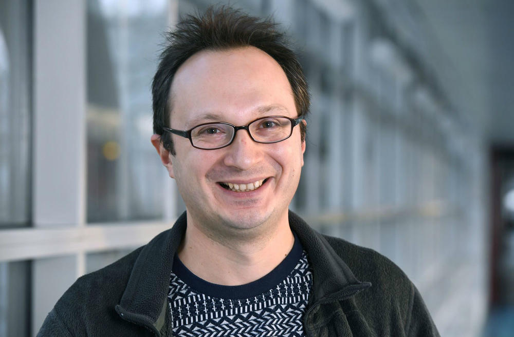
Kirill Bolotin
استاد · Quantum nanoelectronics of 2D materials
Leibniz Institute of Agricultural Development in Transition Economiesمعرفی
Professor Kirill Bolotin is a leading researcher in quantum nanoelectronics of 2D materials at Freie Universität Berlin's Department of Physics. As Principal Investigator for Project B08 within the TRR227 research consortium, he directs the Bolotin Lab with a focus on fundamental properties of atomically thin materials and their potential applications in next-generation electronics.
His research spans multiple frontiers in 2D materials science, with particular emphasis on graphene, transition metal dichalcogenides (TMDs), and hexagonal boron nitride (hBN). Bolotin's group investigates quantum transport phenomena at ultrahigh carrier densities, develops novel strain engineering techniques to manipulate material properties, and studies excitonic physics in monolayer semiconductors. Their work combines advanced nanofabrication with low-temperature electrical measurements, optoelectronic characterization, and nanomechanical testing.
Analysis of recent publications reveals a strong focus on strain-engineered 2D materials, exciton physics in TMDs, and quantum transport phenomena. The group has made significant contributions to understanding how mechanical strain affects electronic properties, how excitons behave in non-uniform environments, and how to achieve ultra-high electrical fields in 2D systems.
Bolotin actively mentors numerous PhD students and has built a substantial research team with expertise spanning nanofabrication, electrical transport, and optical characterization. His laboratory operates the Nanofab facility at Altensteinstraße 23a, equipped with electron beam lithography, focused ion beam systems, and various deposition and characterization tools.
The Bolotin Lab maintains a dedicated cleanroom facility (Nanofab) with comprehensive nanofabrication capabilities including electron beam lithography, metal evaporation, plasma etching, and atomic force microscopy. Their measurement capabilities include cryogenic systems down to 1.5K with 12 Tesla magnets, custom photocurrent setups, and low-temperature photoluminescence/Raman systems, enabling comprehensive characterization of quantum phenomena in 2D materials.