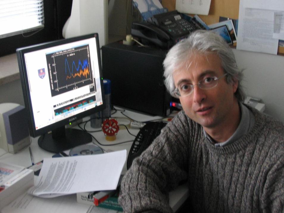
Carles Navau Ros is a Professor in the Department of Physics at Universitat Autònoma de Barcelona (UAB), leading the Group of smart nanoengineered materials, nanomechanics and nanomagnetism (Gnm3). His academic journey includes a PhD in Physics (2000) and a postdoctoral position (1995-1996) at UAB. Research focuses on superconductivity, quantum magnetomechanics, and magnetic nanomaterials. Notable projects include SKYRMIONIC BITS (2024-2027) exploring skyrmionic computing and MetaMagIC (2021-2025) developing magnetic metasurfaces for sustainable tech. Recent work involves magnetic levitation modeling and enhanced sensor technologies. He has authored over 115 publications, with 2025 works on superconducting flux dynamics and magnetic sensor advancements. Projects often involve international collaborations and EU funding.
Stephen Goodnick is the Hans Fischer Senior Fellow at the Technical University of Munich (TUM) and holds the rank of Professor at Arizona State University (ASU), where he previously served as Chair of the Electrical Engineering Department (1996–2005) and Associate Vice President for Research (2006–2008). Currently, he serves as Deputy Director of ASU LightWorks, focusing on renewable energy research. His academic background includes a Ph.D. from Colorado State University (1983) and Alexander von Humboldt Fellowships (1985–1986) at TUM and the University of Modena. His research spans solid-state device physics , nanoelectronics , and energy conversion , with notable contributions to carrier transport modeling and semiconductor device design. He has authored over 350 publications and is a Fellow of the IEEE. Key awards include the 2013 IEEE Phoenix Section Outstanding Faculty Award and the 2008 Robert M. Janowiak Leadership Award. Goodnick’s work bridges theory and application, addressing challenges in photovoltaics, nanoscale electronics, and high-frequency devices. His focus group at TUM, Nanoscience for Renewable Energy Sources , emphasizes sustainable energy solutions through advanced materials and device engineering. Collaborations include modeling silicon heterojunction solar cells and InGaAs nanowire solar cells, advancing energy efficiency and scalability. His leadership roles in professional organizations such as the IEEE Nanotechnology Council and Eta Kappa Nu reflect his commitment to both research excellence and engineering education.
Andrea Di Cicco is a Full Professor of Physics at the University of Camerino, Italy, leading the Physics Division within the School of Science and Technology. His research focuses on condensed matter physics, X-ray absorption spectroscopy, and materials under extreme conditions. He has held roles including Head of the Physics Division and delegate for international research networks. Di Cicco earned his PhD in Physics from the University of Rome 'La Sapienza' (1991) and has held positions as Researcher (1990), Associate Professor (2000), and Full Professor (2018). His scientific contributions include over 200 publications (h-index 46/49), with notable work on X-ray absorption fine structure (XAFS) and the development of the GnXAS data-analysis method. He has been awarded the Stern Prize by the International X-ray Absorption Society (2015) and is listed among 'Top Italian Scientists'. Research interests span synchrotron radiation, free-electron lasers (FELs), and energy materials. He coordinates projects like TIMEX (exploiting FERMI@Elettra) and led the SIRBATT EU project for Li-ion battery materials. His work involves collaborations at international facilities like ESRF, SSRL, and Elettra. Education: PhD in Physics, University of Rome 'La Sapienza', 1991 MSc in Physics, University of Pisa, 1987 BSc in Physics, University of Pisa, 1984 Key Projects: Coordination of TIMEX project (FERMI@Elettra) European SIRBATT project for Li-ion batteries Leadership in international conferences (XAFS14, LAM14) Grants & Funding: EU Framework Programmes Italian MIUR and national grants (PRIN) ESRF, Soleil, and Elettra facilities His group (XAS Group at Camerino) specializes in structural analysis of materials using advanced X-ray techniques. Di Cicco has advised numerous PhD and master's students, fostering interdisciplinary research in energy, nanomaterials, and extreme conditions.
Prof. David DiVincenzo serves as Director of the Institute for Theoretical Nanoelectronics (PGI-2) and the JARA Institute for Quantum Information (PGI-11) at Forschungszentrum Jülich. His research focuses on quantum computing, superconducting qubits, quantum error correction, and many-body localization. He has contributed to foundational work on quantum hardware design, noise mitigation, and theoretical frameworks for scalable quantum systems. Key research themes include the development of superconducting qubit architectures, analysis of quantum chaos effects, and exploration of topological states in semiconductor materials. His work bridges theoretical insights with practical applications in quantum communication and fault-tolerant computing.
Arjun Dahal is an Associate Professor in the Department of Physics at the University of South Alabama, affiliated with the College of Arts and Sciences. He holds a Ph.D. from the University of South Florida (2015) and an M.S. from the University of Minnesota Duluth (2010). His research focuses on nanotechnology, specifically synthesizing metal oxide nanoparticles to enhance photocatalytic efficiency for clean energy and environmental applications. He explores properties like crystallinity, thermal stability, and interface charge transfer in materials like TiO2 and graphene-based systems. His work includes groundbreaking contributions to graphene-nickel interfaces, 2D dielectric monolayers, and photocatalytic material design. He actively seeks motivated students for collaborative research projects. Dahal’s publications span journals like Nature Nanotechnology , Journal of Physical Chemistry C , and APL Materials , reflecting expertise in nanomaterials, surface chemistry, and energy-related applications.
Swiss Federal Institute of Technology in LausanneSwitzerland
Didem Dede is a researcher at the École polytechnique fédérale de Lausanne (EPFL), affiliated with the School of Engineering and the Institute of Materials, specifically within the Laboratory of Molecular Simulation and Catalysis (LMSC). Her work focuses on the synthesis, characterization, and application of two-dimensional materials for advanced technological applications. Research Interests: Dr. Dede's research spans materials science and nanotechnology, with a strong emphasis on 2D materials such as transition metal dichalcogenides, black phosphorus, and hexagonal boron nitride. Her work integrates experimental synthesis with atomic-scale characterization and computational modeling to explore electronic, optical, and catalytic properties. Her investigations into strain engineering, defect dynamics, phase transitions, and heterostructure interfaces contribute to fundamental understanding and practical development in nanoelectronics, energy conversion, and quantum materials. Publication Trends: Her recent publications (2019–2024) reveal a consistent focus on the electronic and structural properties of 2D semiconductors. Themes include carrier mobility modulation, excitonic behavior, interfacial engineering, and scalable synthesis methods. The work is frequently published in high-impact journals such as Nano Letters and ACS Applied Nano Materials , reflecting strong contributions to the nanomaterials community. Scientific Funding: Her research has been supported by major funding bodies, including: Swiss National Science Foundation NCCR QSIT (National Centre of Competence in Research Quantum Science and Technology) CIME (Interdisciplinary Center for Electron Microscopy) EPSRC European Cooperation in Science and Technology Advising and Collaboration: While formal advisees are not listed, her co-authorship on a doctoral thesis and frequent collaboration with leading scientists such as Anna Fontcuberta i Morral and Nicholas Morgan suggests active mentorship and integration within EPFL’s research ecosystem. She contributes to collaborative projects involving advanced microscopy, quantum materials, and energy applications. Laboratories and Facilities: Dr. Dede operates within the LMSC at EPFL, leveraging state-of-the-art facilities such as CIME-GE for electron microscopy and materials characterization. Her access to cleanroom environments and computational resources enables a multidisciplinary approach combining synthesis, experimentation, and simulation.
Swiss Federal Institute of Technology in LausanneSwitzerland
Jean-Michel Sallese is a Senior Researcher at École polytechnique fédérale de Lausanne (EPFL), affiliated with multiple units including the Group of Semiconductor Devices (GR-SCI-IEL) , SEL-ENS , and EDMI-GE . His work focuses on semiconductor device modeling, biosensors, radiation effects in electronics, and microfluidic systems. Research Areas: Field Effect Transistor (FET) physics and modeling Radiation-induced soft errors in integrated circuits High-energy particle solid-state sensors Nanowire and junctionless FET biosensors Microfluidic mixer modeling Recent publications highlight advancements in ISFET biosensors , radiation-hard CMOS , and negative capacitance FETs , with applications spanning medical diagnostics, high-energy physics, and industrial monitoring. He supervises PhD students and co-developed the EDLAB initiative for device modeling. Teaching includes core electronics courses and specialized topics like Modeling Micro-/Nano-Field Effect Devices . No scientific awards are explicitly mentioned in the provided texts.
Professor David Wright is a leading academic in the Department of Engineering at the University of Exeter, where he holds the Chair in Electronic and Computer Engineering. He leads major research initiatives in advanced memory and photonic computing technologies and is deeply involved in national and international research strategy. His research focuses on the development of next-generation non-volatile memory devices and active optical metasurfaces, with recent emphasis on neuromorphic computing, in-memory logic, and chalcogenide phase-change materials for applications in LIDAR, multispectral imaging, and optical computing. His work bridges electronics, materials science, photonics, and artificial intelligence. Professor Wright has led high-impact projects such as the €4 million H2020 Fun-COMP initiative and the EPSRC APT-NuCOM project, collaborating with institutions like Oxford, Muenster, IBM, IMEC, and Microsoft. He is Co-Director of Exeter’s Centre for Doctoral Training in Metamaterials and leads the Nano Engineering Science and Technology Group. He is a Fellow of the IET, has published over 350 papers, holds multiple patents, and has successfully supervised over 50 PhD students. His strategic leadership extends to EU and UK government-level reviews of nanoelectronics programs, including ENIAC and ARTEMIS JTIs. Professor Wright maintains extensive collaborations with global electronics firms such as IBM, Micron, Philips, Sony, and Panasonic, as well as emerging companies like PragmatIC and Bodle Technologies. His work also engages with defense and security sectors. Fellow of the IET He has supervised over 50 PhD students to completion and leads a vibrant research group focused on future computing paradigms. His projects are supported by substantial grants from the EU, EPSRC, and industrial partners. He plays a pivotal role in shaping the future of metamaterials and photonic computing through international collaborations, including a major Centre-to-Centre partnership between Exeter and NSF-funded US centers. Professor Wright is a key figure in Exeter’s Centre for Metamaterials Research & Innovation (CMRI) and contributes to the development of integrated photonic systems for AI, such as in the PHOENICS project. His team explores novel materials and device architectures to enable ultra-fast, low-power computing solutions.
Dr. Ievgeniia Kovalska is a Lecturer in Advanced 2D Energy Materials within the Department of Engineering at the University of Exeter, and a member of the Nano Engineering Science and Technology (NEST) Group and the UK Metamaterials Network. With over a decade of expertise in 2D and carbon materials, her work spans synthesis, characterisation, and applications in energy, (bio)sensing, (opto)electronics, wearables, and sustainable devices. Education: PhD in Chemistry, Chuiko Institute of Surface Chemistry, National Academy of Sciences of Ukraine MSc in Chemistry and Biology, National Pedagogical Dragomanov University, Kyiv BSc in Biology, National Pedagogical Dragomanov University, Kyiv Her research focuses on innovative materials for energy storage (Li-/non-Li batteries) and renewable energy (triboelectric nanogenerators), leveraging graphene, transition metal dichalcogenides, pnictogens, and tetrels. She employs interdisciplinary methods in material synthesis, device fabrication, and testing to advance sustainable technologies. Her work combines fundamental science with practical applications in sensing and energy harvesting. The 15 most recent articles reflect a strong trend in functional 2D materials, with emphasis on energy storage, optoelectronics, sensing, and sustainability. Keywords span materials science, nanotechnology, and engineering, while subfields include graphene applications, TMDCs, flexible devices, and hydrophobic coatings. Her publications demonstrate a consistent focus on scalable synthesis, device integration, and real-world impact. Scientific Awards and Recognition: Over 50 high-ranking publications with 900+ citations and an h-index of 16 Three granted patents, including a novel method for 2D material synthesis Sole inventor of a hydrophobic coating for stone-wall protection Recognition from global research community and media Dr. Kovalska is actively involved in research supervision (PhD and Masters), consultancy, peer review, and external examining. She has received funding for her postdoctoral and current research roles and is committed to advancing diversity in STEM through initiatives like 'Women in Smart Nanomaterials Technology', 'It's Her', and 'Soapbox Science Exeter'. She serves on the Wellbeing, Inclusion, and Culture Committee, promoting equity and inclusion in science. She leads projects on sustainable energy devices and participates in collaborative networks such as the UK Metamaterials Network. Her lab work involves the NEST Group, where she develops hybrid material systems for next-generation technologies. Future work aims to expand the application of 2D materials in climate-responsive and wearable systems.
apl. Prof. Dr. Helmut Karl is a faculty member in the Institute of Physics at the University of Augsburg, within the Faculty of Mathematics, Natural Sciences, and Materials Engineering. He leads the Nanoscale Functional Oxides research group under Experimental Physics IV, focusing on advanced materials synthesis and characterization. Research Interests: His work spans condensed matter physics , nanomaterials , and functional oxides , with a strong emphasis on ion beam synthesis , thin film growth , and semiconductor nanocrystals . He investigates materials such as vanadium dioxide (VO₂), titanium dioxide (TiO₂), and cobaltates for applications in optoelectronics, thermoelectrics, and corrosion protection. The recent publications (2020–2023) reflect a consistent focus on phase-change materials, particularly VO₂, for tunable photonics and thermochromic devices. Additional themes include ion-implanted semiconductors, thermoelectric oxides, and protective coatings, demonstrating a multidisciplinary approach combining materials synthesis, structural analysis, and functional characterization. Scientific Recognition: No specific scientific awards are listed in the provided text. Advising and Grants: While specific students and grant details are not mentioned, Helmut Karl has led long-term research projects and published extensively with collaborators across Germany and internationally, indicating sustained funding and mentorship roles. Laboratory and Equipment: His team utilizes advanced facilities including a Tandem-Ion-Accelerator, molecular-beam epitaxy setups, SQUID-VSM, MOKE magnetometry, and various spectroscopic and electrical characterization tools, supporting a robust experimental program in nanoscale functional materials.
Abde Shafi is a Postdoctoral Researcher in the Department of Electronics and Nanoengineering at Aalto University, affiliated with the Harri Lipsanen Group. He holds a Doctoral degree in Engineering and Technology from Aalto University (awarded December 31, 2023) and a Master's degree in Natural Sciences from the University of Eastern Finland (awarded June 29, 2018). Doctoral degree, Engineering and Technology, Aalto University (2023) Master's degree, Natural Sciences, University of Eastern Finland (2018) His research lies at the intersection of nanoelectronics and optoelectronics, focusing on two-dimensional materials such as MoS₂ and MoTe₂, heterojunction engineering, and the development of high-performance photodetectors and miniaturized spectrometers. His work integrates novel materials like carbon nanotubes and van der Waals tunnel diodes to enhance device functionality and sensitivity. The recent articles highlight a strong trend in developing next-generation optoelectronic devices, especially broadband and miniaturized spectrometers, reconfigurable logic systems, and high-sensitivity photodetectors. These works span disciplines in materials science, electronic engineering, and nanotechnology, with applications in sensing, imaging, and optical computing. Scientific recognition includes the completion of his doctorate and co-authorship on a patent. His research has been disseminated through high-impact journals and shared via public datasets. Abde Shafi actively collaborates within a large research network, contributing to multi-investigator projects and advising is not applicable at this stage. He has contributed to research data and software outputs, including open-access datasets on Dryad and Zenodo, supporting reproducibility and further innovation. He is part of the Harri Lipsanen Group at Aalto University, a research team focused on advanced semiconductor materials and nanoelectronic devices, fostering interdisciplinary collaboration and innovation in nanotechnology and optoelectronics.
M.H. Siekman is a Researcher at the MESA+ Institute specializing in nanoscale characterization within the Nano Electronics Physics of Interfaces and Nanomaterials group. His work focuses on advanced scanning probe microscopy techniques to investigate electronic and mechanical properties of surfaces and nanomaterials at atomic resolution, with particular expertise in scanning tunneling microscopy (STM) methodologies. Siekman's research spans nanomaterials, surface physics, and nanoelectronics, emphasizing high-resolution mapping of electronic properties through innovations like dual modulation STM. His investigations frequently target gold surfaces, self-assembled monolayers, and 2D materials such as graphene, exploring work function modulation, conductivity mapping, and friction phenomena at the nanoscale. This work bridges fundamental surface science with applications in molecular electronics and nanodevice development. Analysis of his 2018-2021 publications reveals a cohesive research trajectory centered on scanning probe techniques, with recurring themes in electronic property mapping, molecular surface modification effects, and 2D material mechanics. His collaborative approach is evident through consistent co-authorship with MESA+ Institute colleagues across diverse surface characterization projects. No scientific awards were documented in the provided materials. While student mentorship and grant details were not explicitly referenced, Siekman maintains active research leadership through his publication record and conference presentations, including invited talks on magnetic force microscopy and thermovoltage measurements. He operates within the Nano Electronics Physics of Interfaces and Nanomaterials research group at the MESA+ Institute, where his work integrates scanning probe methodologies with nanomaterial characterization to advance understanding of surface electronic phenomena and interfacial properties for next-generation nanoelectronic applications.
Dr. Frank Matthes is a Scientific Staff member at Forschungszentrum Jülich GmbH, affiliated with the Peter Grünberg Institute (PGI) and its Electronic Properties (PGI-6) department. His work focuses on theoretical and computational aspects of electronic properties in materials.
Mohammed Qahosh serves as a Researcher within the Electronic Properties group (PGI-6) at the Peter Grünberg Institute, Jülich Research Centre. His role contributes to the institute's core mission of advancing quantum materials research and nanoelectronic technologies through fundamental investigations of material properties. His research spans Condensed Matter Physics and Materials Science with specialized focus on electronic structure analysis, nanoscale electronic phenomena, and semiconductor device physics. This work targets the development of novel electronic materials for next-generation computing and energy applications, emphasizing experimental characterization of quantum material behaviors. As part of PGI-6, Qahosh operates within Jülich's integrated research ecosystem, utilizing advanced facilities including neutron scattering and electron microscopy infrastructure. His collaborative work supports the Helmholtz Association's strategic objectives in quantum technologies and sustainable information systems through interdisciplinary projects across energy and information research domains.
Dr. Dan Mihai Buca serves as a Group Leader in the Semiconductor Nanoelectronics department (PGI-9) at the Peter Grünberg Institute, Forschungszentrum Jülich. His primary research areas encompass: Nanoelectronics Semiconductor Physics Quantum Transport Phenomena Nanotechnology Electronic Materials Science Dr. Buca's research focuses on the design, fabrication, and characterization of semiconductor nanostructures for quantum computing applications and next-generation electronic devices. His work integrates experimental nanofabrication with theoretical modeling to investigate quantum effects in low-dimensional systems, contributing to advancements in quantum information processing. As part of the Peter Grünberg Institute—a leading center for quantum materials research within Europe's largest interdisciplinary research campus—Dr. Buca operates within a collaborative ecosystem featuring state-of-the-art cleanroom facilities and specialized instrumentation for materials synthesis and analysis. The institute's structure includes 15 specialized groups spanning quantum theory, nanoelectronics, and neuromorphic computing, with PGI-9 specifically dedicated to semiconductor device development.