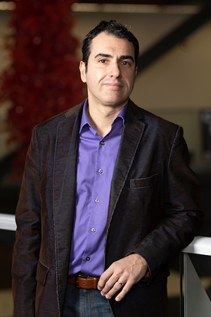
Deep JariwalaView profile
Associate Professor
Deep Jariwala is an Associate Professor and the Peter and Susanne Armstrong Distinguished Scholar at the University of Pennsylvania, with primary appointment in the Department of Electrical and Systems Engineering and secondary affiliation in Materials Science and Engineering. He serves as the Undergraduate Chair for ESE and leads the Device Research and Engineering Laboratory. Dr. Jariwala's research focuses on nanometer and atomic scale devices, materials and interfaces for computing, sensing, information technology, and renewable energy applications. His interdisciplinary work bridges Electrical Engineering, Materials Science, Condensed Matter Physics, Optics, and Physical Chemistry. Key research areas include nanoelectronics, nanophotonics, 2D materials (particularly transition metal dichalcogenides), ferroelectric devices (especially AlScN-based systems), and advanced nanofabrication techniques. His laboratory investigates fundamental properties while developing practical device applications. Analysis of Dr. Jariwala's recent publications (2023-2025) reveals a strong emphasis on wafer-scale 2D materials growth, ferroelectric memory devices, and high-temperature electronics. His work spans from fundamental materials science to device applications, with particular focus on selector-free memory architectures, high-temperature operation (>500°C), and novel approaches to doping and contact engineering in 2D semiconductor devices. Recent trends show increasing emphasis on AI hardware and energy-efficient computing paradigms. Dr. Jariwala has been recognized with the Peter and Susanne Armstrong Distinguished Scholar award for his research contributions. As an academic advisor, Dr. Jariwala mentors undergraduate, graduate, and postdoctoral researchers in his laboratory. His team develops expertise in semiconductor processing, thin film deposition, nanofabrication, electrical characterization, and optical spectroscopy. He actively recruits students interested in nanoelectronics, nanophotonics, and atomic scale materials, providing hands-on experimental experience with close mentoring. The Device Research and Engineering Laboratory, located at 204 Singh Building (3205 Walnut Street), is equipped for advanced materials synthesis, device fabrication, and comprehensive electrical and optical characterization of nanoscale systems.